Friday, 7 December 2012

Hardware Interrupts in 8085......(Interrupts Contd)........


Hardware Interrupt:-
As i have already discussed that there are 6 interrupt pins in the microprocessor used as Hardware Interrrupts given below:
TRAP
RST7.5
RST6.5
RST5.5
INTR
INTA is not an interrupt. INTA is used by the Microprocessor for sending
 the acknowledgement. TRAP has highest priority and RST7.5 has second highest priority and so on.
The Vector address of these interrupts are given below:
                                          
1.TRAP:-It is non maskable edge and level triggered interrupt. TRAP has the highest priority and vectores interrupt. Edge and level triggered means that the TRAP must go high and remain high until it is acknowledged. In case of sudden power failure, it executes a ISR and send the data from main memory to backup memory.
As we know that TRAP can not be masked but it can be delayed using HOLD signal.
This interrupt transfers the microprocessor's control to location 0024H.
How a TRAP interrupt may be masked???
TRAP interrupts can only be masked by reseting the microprocessor. There is no other way to mask it.

2.RST7.5:-It has the second highest priority. It is maskable and edge level triggered interrupt. The vector address of this interrupt is 003CH. Edge sensitive means input goes high and no need to maintain high state until it is recognized.
How It may be masked??
It can also be reset or masked by reseting microprocessor. It can also be resetted by DI instruction.

3.RST6.5 and RST5.5:-These are level triggered and maskable interrupts. When RST6.5 pin is at logic 1, INTE flip-flop is set. RST 6.5 has third highest priority and RST 5.5 has fourth highest priority.
It can be masked by giving DI and SIM instructions or by reseting microprocessor.


4.INTR:-It is level triggered and maskable interrupt. It has the lowest priority. It can be disabled by reseting the microprocessor or by DI and SIM instruction.


The following sequence of events occurs when INTR signal goes high:
1. The 8085 checks the status of INTR signal during execution of each instruction.

2. If INTR signal is high, then 8085 complete its current instruction and sends active low interrupt acknowledge signal, if the interrupt is enabled.

3.On receiving the instruction, the 8085 save the address of next instruction on stack and execute received instruction.

Software Interrupts in 8085.....(Interrupt Contd..)


Software Interrupts:-
A software interrupts is a particular instructions that can be inserted into the desired location in the rpogram. There are eight Software interrupts in 8085 Microprocessor. From RST0 to RST7.


RST0
RST1
RST2
RST3
RST4
RST5
RST6
RST7


They allow the microprocessor to transfer program control from the main program to the subroutine program. After completing the subroutine program, the program control returns back to the main program.


We can calculate the vector address of these interrupts using the formula given below:
                        
                             Vector Address = Interrupt Number * 8
So we can find simply vector address. For Example:


RST2:        vector address=2*8    =  16
RST1:        vector address=1*8    =  08
RST3:        vector address=3*8    =  24


Vector address table for the software interrupts:


Interrupts in 8085 Microprocessor


First of all i want to discuss that what is Interrupt???????

Interrupt is a mechanism by which an I/O or an instruction can suspend the normal execution of processor and get itself serviced. Generally, a particular task is assigned to that interrupt signal. In the microprocessor based system the interrupts are used for data transfer between the peripheral  devices and the microprocessor. The processor will check the interrupts always at the 2nd T-state of last machine cycle.

Interrupt Service Routine(ISR):-A small program or a routine that when executed services
 the corresponding interrupting source is called as an ISR.

Maskable/Non-Maskable Interrupt:-An interrupt that can be disabled by writing some instruction is known as Maskable Interrupt otherwise it is called Non-Maskable Interrupt.

There are two types of interrupts used in 8085 Microprocessor:

1.Hardware Interrupts
2.Software Interrupts

There are 6 pins available in 8085 for interrupt:

TRAP
RST 7.5
RST6.5
RST5.5
INTR
INTA

Execution of Interrupts:-
When there is an interrupt requests to the Microprocessor then after accepting the interrupts Microprocessor send the INTA (active low) signal to the peripheral. The vectored address of particular interrupt is stored in program counter. The processor executes an interrupt service routine (ISR) addressed in program counter.

Memory Interfacing Using RAM and ROM both with 8085 Microprocessor


Interfacing RAM and ROM both at a time with 8085:


Here ROM with 32 kb and RAM with 64kb has been used.


32kb = 32768bytes   is equal to 
2^15 

and


64kb = 65536bytes  is equal to 2^16 


So it is clear that 15 address lines are required for interfacing of ROM and 16 address lines are required for interfacing of RAM. As we know that there are only 16 address lines in 8085 Microprocessor. But we need 16+15 = 31 lines.


Think!!!!!!!!


How it may be possible???

Memory Interfacing in 8085 Microprocessor


Memory Interfacing:-As we know that any system which process digital data needs the facility for storing the data. Interfacing is a technique to be used for connecting the Microprocessor to Memory.


Now a days Semiconductor memories are used for storing purpose. There are some of the advantages of the
 semiconductor memory.


Small size
High speed
Better reliability
Low cost


Generally, RAM or ROM is used for memory interfacing.


Memory:-A memory is a digital IC which stores the data in binary form.


Memory Size:-The number of location and number of bits per word will vary from memory to memory. For example, If a particular memory chip is capable of storing M words with each word having N-bits. Then the size of the memory will be M× N.


Interfacing a ROM memory of 4096*8 with 8085 Microprocessor:-


Given memory size = 4096 * 8
4096 =2^12.
So 12 lines will be used for interfacing. A0 to A11


In this system A0 to A11 lines of Microprocessor will be connected to the address lines of the memory. and D0 to D7 of the 8085 microprocessor will be connected to the data bus of the memory.
As we know that the it is EPROM, so only RD pin is connected to the microprocessor. There is not the facility for writing data.


In case if you are using RAM then you have to connect one more pin for writing operation.


As you can see that there is a pin named CS. Generally this pin is used for Selction for the chip in case of two or more than memory chip. 
Latch has been used to separate the data and address bus.

Representation of signals in Timing Diagram Of 8085


1.Clock Signals:-As we know that the microprocessor operates with reference to clock signals provided to it. At pins X1 and X2 we provide clock signals and this frequency is divided by two. This frewuency is called as the operating frequency.


2.Single Line Signal:-The status of single line will be either LOW or HIGH. But the change from one state to another state is not possible in zero time.


3.Multiple Line Signals:-In Microprocessor we have multiple lines. These signals are also called as bus signals. If a single line changes occure then we have to show a crossing to indicate change in contents.

Some Short Questions Self Test


Q>Differentiate between Microprocessor and Microcomputer?


Q>What is an interrupt?


Q>Draw and explain the block diagram of 8085.


Q>List the function of ALU.


Q>What is the function 
of READY Pin?


Q>List the name of interrupt signal in 8085.


Q>What is the need of demultiplexing of address bus and data bus in 8085?


Q>A processor has 16 MB memory, how many address lines are required to access this memory.


Q>Add the two hex number 24H and FFH. and also tells about the flag status.


Q>Why are the AD0-AD7 lines multiplexed?


Q>Name the register pair that can be used for 16 bits data.


Q>Define the signals used in 8085 microprocessor.

How to Demultiplex Address and Data Bus


Generally, 74LS373 Latch IC is used for latching the address issued by Microprocessor.
It has 8-latches(D-flip flop).


Address will
 appear on AD0-AD7 lines.
ALE will go high and forcing enable G pin of Latch. This will make the latch transparent. It means whatever will be input, will be output. Presently input address is A0-A7.Therefore output is A0-A7.
When ALE=0, then AD0-AD7 will now be used as data bus.

All Addressing Modes in 8085 Microprocessor With Example


Addressing Modes in 8085
There are five addressing modes in 8085.

1. Immediate Addressing Mode: - An immediate is transferred directly to the register.

Eg: - MVI A, 30H (30H is copied into the register A)

          MVI B,40H(40H is copied into the register B).


2. Register Addressing Mode: - Data is copied from one register to another register.

Eg: - MOV B, A (the content of A is copied into the register B)

          MOV A, C (the content of C is copied into the register A).


3. Direct Addressing Mode: - Data is directly copied from the given address to the register.

Eg: - LDA 3000H (The content at the location 3000H is copied to the register A).


4. Indirect Addressing Mode: - The data is transferred from the address pointed by the data in a register to other register.

Eg: - MOV A, M (data is transferred from the memory location pointed by the regiser to the accumulator).


5.Implied Addressing Mode: - This mode doesn't require any operand. The data is specified by opcode itself.

Pin Diagram of 8085 Microprocessor with Description


8085 is a general purpose microprocessor having 40 pins and works on single power supply. To study the pin diagram we group
 the signals into 5 categories:

1.Power Supply
2.Clock Signals
3.Interrupt Signals
4.Address and Data bus
5.Control and Status signals
6.Serial I/O Port
7.DMA Request Signals


Power Supply Signal and clock signal:
VCC:-Vcc is to be connected to +5V power supply.
Vss:-Ground reference
X1 and X2:- This pin is used for providing the clock frequency to the microprocessor. Generally Crystal oscillator or LC oscillator is used to generate the frequency. The frequency generated here is internally divided into two.As we know that the basic operating timing frequency of the microprocessor is 3 MHz so 
6 MHz frquency is applied.


Serial Input Output port:-
SID and SOD:-These pins are used for serial data communication.


Interrupt Signal:-
Pin 6 to 11:- These pins are used for interrupt signals. Generally and external devices are connected here which requests the microprocessor to perform a particular task.

There are 5 pins for hardware interrupts-
TRAP, RST7.5, RST 6.5, RST5.5 and INTR
INTA is used for acknowledgement. Microprocessor sends the acknowledgement to external devices through the INTA pin.


Address Bus and DATA Buses:-
AD0-AD7:-These are multiplexed address and data bus. So it can be used to carry the lower order 8 bit address as well as the data. Generally these lines are demultiplexed using the Latch.
During the opcode fetch operation, in the first clock cycle the lines deliever the lower order address bus  A0-A7.
In the subsequent IO/M read or write it is used as data bus D0-D7. CPU can read or write data through these lines.

A8-A15:- These are address bus used to address the memory location.


Control And Status Signal:-
S0 and S1:-It is used for the status signal in microprocessor.

ALE(Airthmetic Latch Enable):-This signal is used to capture the lower address presented on multiplexed address and data bus.

RD:-This is active low input generally
 used for reading operation.

WR:-This is active low input used for writing operation.

IO/M:-This pin is used to select the memory or input-output through which we want to communicate the data.

READY:-As we know that memory and input -output have slower response than microprocessor. So a microprocessor may now be able to handle further data till it completes the present job. So it is in waiting state. As it completes the present job it sets the READY pin. Microprocessor enters into wait state while READY pin is disabled.
RESET IN:-This is active low input. This pin is used to reset the microprocessor. An active low signal applied to this pin reset the program counter inside the microprocessor. The busses are tristated.
RESETOUT:-If we want to reset the external devices connected to the microprocessor then a signal applied to this pin resets the external devices.


DMA Request Signal:
HOLD and HLDA:-HOLD is an active high input signal used by the other controller to request microprocessor about use of address, data and control signal. The HOLD and HLDA signal are used for direct memory access(DMA). DMA controller receives a requests from a device and in turn issues the HOLD signal to the microprocessor.
The processor releases the system bus and then acknowledges the HOLD signal with HLDA signal. The DMA transfer thus begins.

Microcomputers and Microprocessor


Microcomputer:-Microcomputers are much smaller computer. They operate still more slowly and they work with still smaller data words (typically 4 bits, 8 bits, 16 bits or 32 bits).
They can address few thousands to
 few million memory location. One of the important feature of microcompter is that the CPU is usually a single IC called as a microprocessor.


Difference b/w Microprocessor and microcomputer:

1. A microprocessor has a CPU to which we have to add ROM, RAM and  ports to make a microcomputer.
2.Application of microcomputer are from sewing machine, washing machine and other domestic appliances to computer added design system.
3.Intel 8051 is a microcomputer which is actually a single chip computer.

Difference Between Address Bus vs Data Bus of 8085 Microprocessor


According to computer architecture, a bus is defined as a system that transfers data between hardware components of a computer or between two separate computers. Initially, buses were made up using electrical wires, but now the term bus is used more broadly to identify any physical subsystem that provides equal functionality as the earlier electrical buses. Computer buses can be parallel or serial and can be connected as multidrop, daisy chain or by switched hubs. System bus is a single bus that helps all major components of a computer to communicate with each other. It is made up of an address bus, data bus and a control bus. The data bus carries the data to be stored, while address bus carries the location to where it should be stored.

Address Bus

Address bus is a part of the computer system bus that is dedicated for specifying a physical address. When the computer processor needs to read or write from or to the memory, it uses the address bus to specify the physical address of the individual memory block it needs to access (the actual data is sent along the data bus). More correctly, when the processor wants to write some data to the memory, it will assert the write signal, set the write address on the address bus and put the data on to the data bus. Similarly, when the processor wants to read some data residing in the memory, it will assert the read signal and set the read address on the address bus. After receiving this signal, the memory controller will get the data from the specific memory block (after checking the address bus to get the read address) and then it will place the data of the memory block on to the data bus.
The size of the memory that can be addressed by the system determines the width of the data bus and vice versa. For example, if the width of the address bus is 32 bits, the system can address 232 memory blocks (that is equal to 4GB memory space, given that one block holds 1 byte of data).

Data Bus

A data bus simply carries data. Internal buses carry information within the processor, while external buses carry data between the processor and the memory. Typically, the same data bus is used for both read/write operations. When it is a write operation, the processor will put the data (to be written) on to the data bus. When it is the read operation, the memory controller will get the data from the specific memory block and put it in to the data bus.

What is the difference between Address Bus and Data Bus?
Data bus is bidirectional, while address bus is unidirectional. That means data travels in both directions but the addresses will travel in only one direction. The reason for this is that unlike the data, the address is always specified by the processor. The width of the data bus is determined by the size of the individual memory block, while the width of the address bus is determined by the size of the memory that should be addressed by the system.


Bus Structure Of 8085 Microprocessor


There are three buses in Microprocessor:
1.Address Bus
2.Data Bus
3.Control Bus


1.Address Bus:-Genearlly, Microprocessor has 16 bit address bus. The bus over which the CPU sends out the address of the memory location is known as Address bus. The address bus carries the address of memory location to be written or to be read from.
The address bus is unidirectional. It means bits flowing occurs only in one direction, only from microprocessor to peripheral devices.
We can find that how much memory location it can using the formula 2^N. where N is the number of bits used for address lines.

here,    2^16 = 65536bytes or 64Kb
So we can say that it can access upto 64 kb memory location.

Q.>If a processor has 4 GB memory then how many address lines are required to access this memory?

Ans: 4GB= 4 * 1GB

         4 = 2^2
        
         1GB = 2^30
        
          4GB = 2^2   *   2^30 = 2^32

          So 32 address lines are required to access the 4 GB memory.


2.Data Bus:-8085 Microprocessor has 8 bit data bus. So it can be used to carry the 8 bit data starting from 00000000H(00H) to 11111111H(FFH). Here 'H' tells the Hexadecimal Number. It is bidirectional. These lines are used for data flowing in both direction means data can be transferred or can be received through these lines. The data bus also connects the I/O ports and CPU. The largest number that can appear on the data bus is 11111111.

It has 8 parallel lines of data bus. So it can access upto 2^8 = 256 data bus lines.

3.Control Bus:-The control bus is used for sending control signals to the memory and I/O devices. The CPU sends control signal on the control bus to enable the outputs of addressed memory devices or I/O port devices.

Some of the control bus signals are as follows:
1.Memory read
2.Memory write
3.I/O read
4.I/O write.

Architecture Diagram of 8085 Microprocessor


This is the functional block diagram of the 8085 Microprocessor.


This is the function
al Block Diagram of 8085 Microprocessor.

Acumulator:-It is a 8-bit register which is used to perform airthmetical and logical operation. It stores the output of any operation. It also works as registers for i/o accesses.

Temporary Register:-It is a 8-bit register which is used to hold the data on which the acumulator is computing operation. It is also called as operand register because it provides operands to ALU.

Registers:-These are general purposes registers. Microprocessor consists 6 general purpose registers of 8-bit each named as B,C,D,E,H and L.   Generally theses registers are not used for storing the data permanently. It carries the 8-bits data. These are used only during the execution of the instructions.
These registers can also be used to carry the 16 bits data by making the pair of 2 registers. The valid register pairs available are BC,DE HL. We can not use other pairs except BC,DEand HL. These registers are programmed by user.


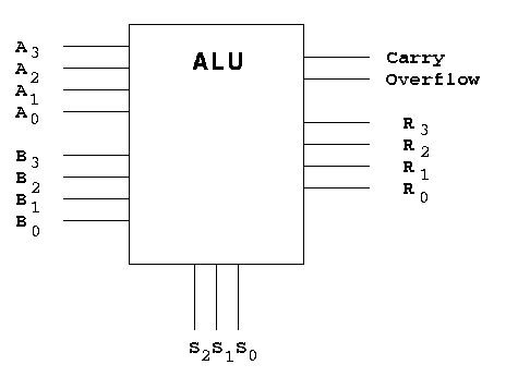
ALU:-ALU performs the airthmetic operations and logical operation.

Flag Registers:-It consists of 5 flip flop which changes its status according to the result stored in an accumulator. It is also known as status registers. It is connected to the ALU.
There are five flip-flops in the flag register are as follows:
1.Sign(S)
2.zero(z)
3.Auxiliary carry(AC)
4.Parity(P)
5.Carry(C)
The bit position of the flip flop in flag register is:


All of the three flip flop set and reset according to the stored result in the accumulator.
1.Sign- If D7 of the result is 1 then sign flag is set otherwise reset. As we know that a number on the D7 always desides the sign of the number.
if D7 is 1: the number is negative.
if D7 is 0: the number is positive.

2.Zeros(Z)-If the result stored in an accumulator is zero then this flip flop is set otherwise it is reset.

3.Auxiliary carry(AC)-If any carry goes from D3 to D4 in the output then it is set otherwise it is reset.

4.Parity(P)-If the no of 1's is even in the output stored in the accumulator then it is set otherwise it is reset for the odd.

5.Carry(C)-If the result stored in an accumulator generates a carry in its final output then it is set otherwise it is reset.

Instruction registers(IR):-It is a 8-bit register. When an instruction is fetched from memory then it is stored in this register.

Instruction Decoder:- Instruction decoder identifies the instructions. It takes the informations from instruction register and decodes the instruction to be performed.

Program Counter:-It is a 16 bit register used as memory pointer. It stores the memory address of the next instruction to be executed. So we can say that this register is used to sequencing the program. Generally the memory have 16 bit addresses so that it has 16 bit memory.
The program counter is set to 0000H.

Stack Pointer:-It is also a 16 bit register used as memory pointer. It points to the memory location called stack. Generally stack is a reserved portion of memory where information can be stores or taken back together.

Timing and Control Unit:-It provides timing and control signal to the microprocessor to perform the various operation.It has three control signal. It controls all external and internal circuits. It operates with reference to clock signal.It synchronizes all the data transfers.
There are three control signal:
1.ALE-Airthmetic Latch Enable, It provides control signal to synchronize the components of microprocessor.
2.RD- This is active low used for reading operation.
3.WR-This is active low used for writing operation.

There are three status signal used in microprocessor S0, S1 and IO/M. It changes its status according the provided input to these pins.


Serial Input Output Control-There are two pins in this unit. This unit is used for serial data communication.

Interrupt Unit-There are 6 interrupt pins in this unit. Generally an external hardware is connected to these pins. These pins provide interrupt signal sent by external hardware to microprocessor and microprocessor sends acknowledgement for receiving the interrupt signal. Generally INTA is used for acknowledgement. 


Register Section:-Many registers has been used in microprocessor. 


It consists of PIPO(Parallel Input Parallel Output) register.

Applications Of Microprocessor in General Life


There are a lot of applications of Microprocessor in general life.Some of the applications are given below:

Mobile Phones
Digital Watches
Washing Machine
Computer
Lighting Control
Traffic Control
LAPTOP
Modems
Power Stations
Television
CD Player
Multimeter
CRO
Wave generator
More applications in medical

Introduction to Microprocessor


Introduction to Microprocessor

8085 Microprocessor Definition: When we hear the word microprocessor then what comes to our mind is a small (i.e-micro) IC that can process data i.e- perform airthmetic and logical operations. Microprocessor reads the instructions from memory and excutes it line by line.
As we know that all of this operation is performedGenerally all of this operation is done by the ALU unit in Microprocessor.
 by the CPU in a large computer.
So we can compare the CPU and ALU as the fig. given below.

OverviewdiagramofMicroprocessor_thum                     


ALU:-This section is used for performing the airthmetic and logical operation in Microprocessor. Here A and B are the input pins where operands are put on which we want to perform airthmetic and logical operation. A and B section are operand section and it processes it according to the given instruction.


Airthmetic operation:- Like addition, substraction,multipllication,division etc.
Logical Operation:- Like AND,OR,NOT,EX-OR etc all logical operation.
Opcode:- A Binary code that indicates the operation to be performedis called as an opcode.

Operands:- The data on which the operation is to be performed is known as operand.

Instruction:-The combination of opcode and  an operand,that can be used to instruct a system is called as an instruction.

Instruction set:-A list of all the instructions that can be issued to a system is called as instruction set.

Program/Subroutine/Routine:-A set of instructions written in a particular sequence,so as to implement a given task. A subroutine in assembly refers to function as in C/C++.

Bus:-A group of lines, pins or signal s having commons functions is termed as the bus.
There are three buses in 8085 Microprocessor:
1. Data bus- Microprocessor has 8 bit data bus.  It carries data(to receive and to transmit) from memory or to memory.
2. Address bus-Microprocessor has 16 bit address bus. Generally it is used to select the memory or I/O location through which we want to communicate the microprocessor.
3. System bus-It provides control and timing signal to perform the various operation.

Memory:-Generally a memory is used for storage purpose. We can store the data,instruction sets etc. Instruction sets are stored in memory in form of binary number. It provides that information to Microprocessor whenever necessary. Microprocessor reads instructions from memory and performs the operation in its ALU section. Results are transferred to Output Section(LCD display,LED, others). It may also stored in memory as it needs.
There are two types of memory:
RAM(Random Access Memory)- It is a type of memory. it provides the reading and writing both facility.
ROM(Read Only Memory)-Data or program stored in ROM can only be read. It can not be altered. It doesn't provide the writing facility.
 
;